Nanoscale Fabrication and Processing of Next-Generation Semiconductor Materials
Introduction to Advanced Semiconductor Materials
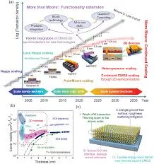
The relentless pursuit of Moore's Law has driven semiconductor technology toward increasingly smaller feature sizes and more complex material systems. Next-generation semiconductor materials represent a paradigm shift from traditional silicon-based technologies, incorporating novel compounds and structures that enable superior electronic, photonic, and quantum properties. These materials include two-dimensional (2D) semiconductors, wide-bandgap semiconductors, and topological insulators, each offering unique advantages for specific applications.
Key Next-Generation Semiconductor Materials
Two-Dimensional Materials
Two-dimensional materials, particularly transition metal dichalcogenides (TMDs) like MoS₂ and WS₂, have emerged as promising candidates for ultra-scaled electronic devices. Their atomic thickness provides excellent electrostatic control, while their unique electronic properties enable novel device functionalities. Graphene, though lacking a bandgap, remains valuable for interconnects and RF applications due to its exceptional carrier mobility.
Wide-Bandgap Semiconductors
Materials such as gallium nitride (GaN) and silicon carbide (SiC) offer superior performance in high-power, high-frequency, and high-temperature applications. Their wide bandgaps enable higher breakdown voltages and improved thermal stability compared to silicon, making them ideal for power electronics, RF amplifiers, and optoelectronic devices.
Topological Insulators and Quantum Materials
Topological insulators represent a class of materials that are insulating in their bulk but conduct electricity on their surface through protected edge states. These materials hold promise for low-power electronics and quantum computing applications, where their unique electronic properties can be harnessed for novel device concepts.
| Material | Bandgap (eV) | Electron Mobility (cm²/V·s) | Thermal Conductivity (W/m·K) | Key Applications |
|---|---|---|---|---|
| Silicon (Si) | 1.12 | 1400 | 150 | Digital logic, memory |
| Gallium Arsenide (GaAs) | 1.42 | 8500 | 55 | RF, optoelectronics |
| Gallium Nitride (GaN) | 3.4 | 2000 | 130 | Power electronics, RF |
| Molybdenum Disulfide (MoS₂) | 1.8 (monolayer) | 200 | 34 | Ultra-scaled transistors |
Advanced Nanofabrication Techniques
Atomic Layer Deposition (ALD)
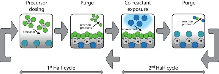
Atomic Layer Deposition has become indispensable for depositing ultra-thin, conformal films with atomic-level precision. ALD enables the fabrication of high-k gate dielectrics, diffusion barriers, and encapsulation layers for next-generation semiconductor devices. The self-limiting nature of ALD reactions ensures excellent thickness control and uniformity, even on high-aspect-ratio structures.
Extreme Ultraviolet Lithography (EUVL)
EUV lithography operating at 13.5 nm wavelength has enabled the continuation of Moore's Law by patterning features below 10 nm. The implementation of EUVL requires sophisticated optics, photoresist chemistry, and mask technology to achieve the necessary resolution and pattern fidelity for advanced semiconductor nodes.
Directed Self-Assembly (DSA)
Directed self-assembly of block copolymers offers a complementary approach to traditional lithography for creating periodic nanostructures. By controlling the molecular weight and composition of block copolymers, features with sub-10 nm dimensions can be achieved with high density and uniformity, potentially reducing fabrication costs for certain applications.
Processing Challenges and Solutions
Interface Engineering
The performance of next-generation semiconductor devices is critically dependent on interface quality. Interface states, defects, and Fermi-level pinning can severely degrade device characteristics. Advanced surface treatments, interfacial layers, and annealing processes are being developed to optimize interface properties and minimize detrimental effects.
Metallization and Contact Formation
Forming low-resistance contacts to novel semiconductor materials presents significant challenges. Fermi-level pinning, Schottky barrier formation, and material interactions must be carefully managed. Alloyed contacts, interlayer engineering, and novel metal schemes are being investigated to achieve ohmic behavior with minimal contact resistance.
| Technique | Resolution | Throughput | Cost | Suitable Materials |
|---|---|---|---|---|
| EUV Lithography | <10 nm | High | Very High | All |
| Electron Beam Lithography | <5 nm | Low | High | All |
| Directed Self-Assembly | 5-20 nm | Medium | Medium | Limited |
| Nanoimprint Lithography | 10-20 nm | High | Low | Limited |
Characterization and Metrology
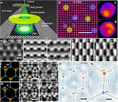
Advanced characterization techniques are essential for understanding and optimizing next-generation semiconductor materials and processes. Transmission electron microscopy (TEM), scanning tunneling microscopy (STM), and various spectroscopic methods provide atomic-scale insights into material structure, composition, and electronic properties. In-line metrology must keep pace with shrinking dimensions, requiring the development of novel measurement techniques with sufficient sensitivity and resolution.
Future Perspectives and Applications
The continued advancement of nanoscale fabrication and processing will enable new computing paradigms beyond traditional CMOS technology. Neuromorphic computing, quantum computing, and heterogeneous integration represent promising directions that leverage the unique properties of next-generation semiconductor materials. The integration of different material systems on a common platform will likely become increasingly important, requiring sophisticated fabrication approaches and interface engineering.
Quantum Device Fabrication
The fabrication of quantum bits (qubits) based on semiconductor materials requires extreme precision and control over material properties and interfaces. Defect engineering, isotopic purification, and advanced patterning techniques are being developed to create qubits with long coherence times and high fidelity operations.
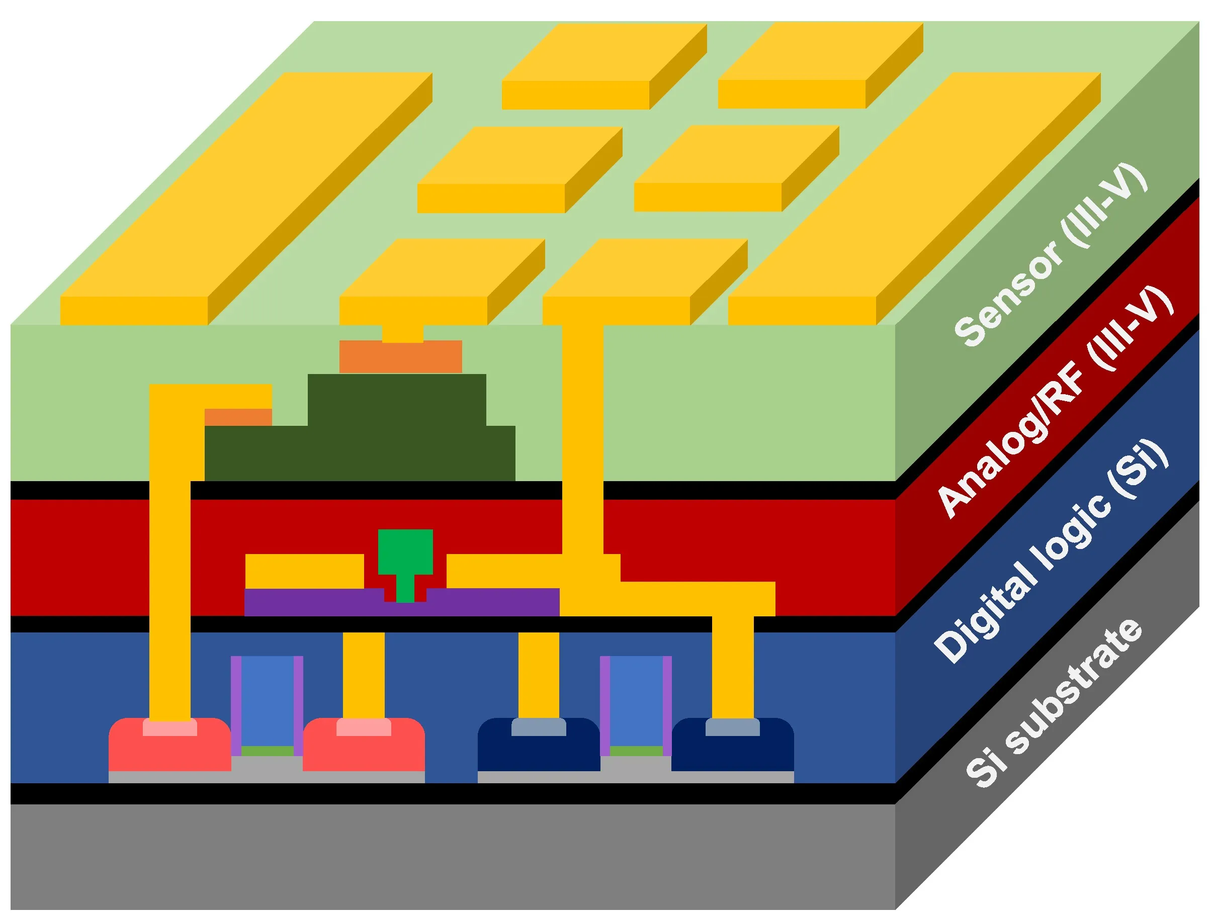
Heterogeneous Integration
The combination of different semiconductor materials on a single chip enables optimized performance for diverse functions. 3D integration, wafer bonding, and selective epitaxy are key technologies for realizing heterogeneous systems that leverage the strengths of multiple material platforms.
Conclusion
Nanoscale fabrication and processing of next-generation semiconductor materials represents a frontier in semiconductor technology that will enable continued performance improvements and new functionality. The successful implementation of these advanced materials requires coordinated advances in materials science, fabrication techniques, characterization methods, and device design. As we approach fundamental physical limits, innovative approaches to materials engineering and processing will become increasingly critical for future technological progress.