Understanding Semiconductor Materials: The Foundation of Modern Electronics
Semiconductor materials represent one of the most important technological discoveries of the 20th century, forming the foundation of modern electronics and digital technology. These unique materials possess electrical properties that sit between conductors and insulators, making them indispensable for controlling and manipulating electrical currents in electronic devices.
The significance of semiconductors cannot be overstated—they power everything from smartphones and computers to medical equipment and renewable energy systems. Understanding what semiconductor materials are, how they work, and why they're so crucial provides insight into the technological world we live in today.
Fundamental Properties of Semiconductors
Electrical Conductivity
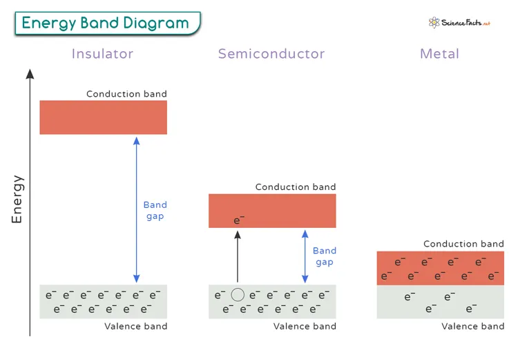
Semiconductors are defined by their unique electrical conductivity, which falls between that of conductors (like copper and aluminum) and insulators (like glass and rubber). This intermediate conductivity can be precisely controlled through various methods, including doping, temperature changes, and light exposure.
Band Gap Theory
The electronic band structure of semiconductors features a crucial energy gap called the "band gap" between the valence band (where electrons are bound to atoms) and the conduction band (where electrons can move freely). This band gap typically ranges from 0.1 to 4 electron volts (eV), allowing semiconductors to function as switches in electronic circuits.
Temperature Dependence
Unlike metals, whose conductivity decreases with rising temperature, semiconductors exhibit increasing conductivity as temperature rises. This occurs because thermal energy helps electrons cross the band gap into the conduction band, creating more charge carriers.
Types of Semiconductor Materials
Elemental Semiconductors
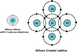
Elemental semiconductors consist of single elements from group IV of the periodic table. Silicon is the most prominent example, accounting for approximately 95% of all semiconductor devices produced worldwide. Germanium was historically important but has been largely replaced by silicon due to its superior properties.
Compound Semiconductors
Compound semiconductors are formed by combining elements from different groups in the periodic table. These materials often offer advantages for specific applications:
| Material Type | Examples | Key Applications | Band Gap (eV) |
|---|---|---|---|
| III-V Compounds | Gallium Arsenide (GaAs), Indium Phosphide (InP) | High-frequency devices, optoelectronics | 1.42 (GaAs) |
| II-VI Compounds | Zinc Selenide (ZnSe), Cadmium Telluride (CdTe) | Solar cells, photodetectors | 2.70 (ZnSe) |
| IV-IV Compounds | Silicon Carbide (SiC) | High-temperature, high-power devices | 2.36-3.23 |
Organic Semiconductors
Organic semiconductors are carbon-based materials that offer flexibility, low-cost manufacturing, and tunable electronic properties through chemical synthesis. While less efficient than inorganic semiconductors, they enable applications like flexible displays and organic solar cells.
Doping and Charge Carriers
The intentional introduction of impurities into pure semiconductor materials, known as doping, is what makes semiconductors so technologically valuable. This process allows precise control over electrical properties.
N-type Semiconductors
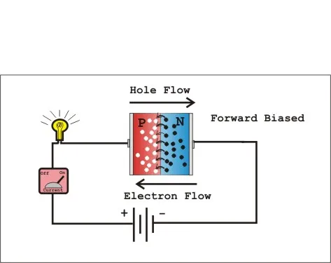
N-type semiconductors are created by doping with donor atoms that have more valence electrons than the host material. For silicon, common n-type dopants include phosphorus and arsenic. These extra electrons become the primary charge carriers, creating materials with excess negative charge carriers.
P-type Semiconductors
P-type semiconductors result from doping with acceptor atoms that have fewer valence electrons than the host material. Boron and gallium are common p-type dopants for silicon. This creates "holes" (absence of electrons) that act as positive charge carriers.
| Doping Type | Dopant Elements (for Silicon) | Charge Carriers | Electrical Behavior |
|---|---|---|---|
| N-type | Phosphorus, Arsenic, Antimony | Electrons (majority), Holes (minority) | Negative charge dominant |
| P-type | Boron, Gallium, Indium | Holes (majority), Electrons (minority) | Positive charge dominant |
Semiconductor Manufacturing Process
Crystal Growth
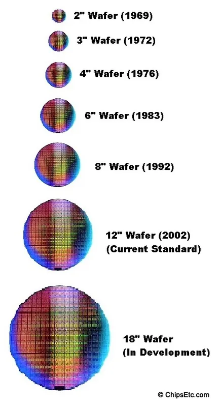
The manufacturing process begins with growing extremely pure single crystals of semiconductor material. The Czochralski process is commonly used for silicon, producing cylindrical ingots that are then sliced into thin wafers.
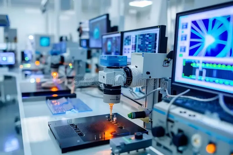
Wafer Processing
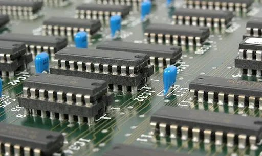
Semiconductor wafers undergo multiple processing steps including oxidation, photolithography, etching, doping, and deposition. These processes create the intricate patterns of transistors and interconnects that form integrated circuits.
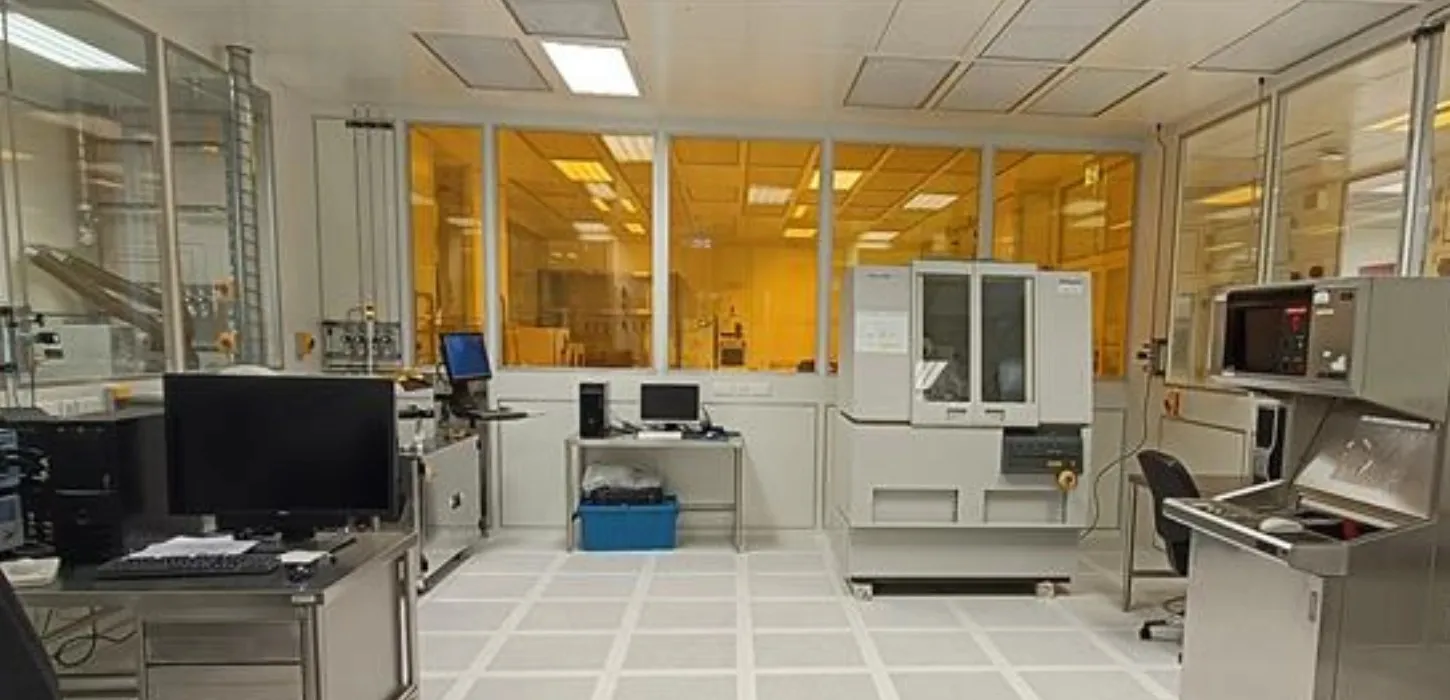
Packaging and Testing
After wafer processing, individual chips are separated, packaged to protect them from environmental factors, and tested to ensure functionality and reliability before being integrated into electronic devices.
Applications of Semiconductor Materials
Digital Electronics
Semiconductors form the basis of all digital electronics, from microprocessors and memory chips to logic gates. The ability to create transistors that can act as switches enables binary computation and data storage.
Power Electronics
Power semiconductors control and convert electrical power in applications ranging from motor drives and power supplies to renewable energy systems and electric vehicles.
Optoelectronics
Semiconductors that interact with light enable technologies including LEDs, laser diodes, photodetectors, and solar cells. Different semiconductor materials are chosen based on their band gap to interact with specific wavelengths of light.
| Application Area | Key Semiconductor Devices | Common Materials Used |
|---|---|---|
| Computing | Microprocessors, Memory chips, GPUs | Silicon, Gallium Arsenide |
| Communications | RF amplifiers, Modulators, Detectors | Gallium Nitride, Silicon Germanium |
| Energy | Solar cells, Power converters, Inverters | Silicon, Gallium Arsenide, Silicon Carbide |
| Sensing | Image sensors, Temperature sensors, Pressure sensors | Silicon, Indium Gallium Arsenide |
Future Developments in Semiconductor Technology
Advanced Materials
Research continues into new semiconductor materials like graphene, transition metal dichalcogenides, and perovskite structures that could enable faster, more efficient, or entirely new types of electronic devices.
Quantum Computing
Semiconductors are playing a crucial role in the development of quantum computing, with silicon quantum dots and superconducting circuits emerging as promising platforms for qubit implementation.
Neuromorphic Computing
Semiconductor devices that mimic the behavior of biological neurons and synapses are being developed for energy-efficient artificial intelligence systems that could revolutionize computing architecture.
Conclusion
Semiconductor materials represent a cornerstone of modern technology, enabling the digital revolution that has transformed society. Their unique electrical properties, combined with our ability to precisely control these properties through doping and fabrication techniques, have made possible everything from personal computers and smartphones to medical imaging systems and renewable energy technologies.
As research continues to push the boundaries of what's possible with semiconductors, these remarkable materials will undoubtedly continue to drive technological innovation for decades to come, enabling new applications we can only begin to imagine today.